JEDEC Publishes GDDR7 Memory Spec: Next-Gen Graphics Memory Adds Faster PAM3 Signaling & On-Die ECC
by Ryan Smith & Anton Shilov on March 6, 2024 9:00 AM EST
JEDEC on Tuesday published the official specifications for GDDR7 DRAM, the latest iteration of the long-standing memory standard for graphics cards and other GPU-powered devices. The newest generation of GDDR brings a combination of memory capacity and memory bandwidth gains, with the later being driven primarily by the switch to PAM3 signaling on the memory bus. The latest graphics RAM standard also boosts the number of channels per DRAM chip, adds new interface training patterns, and brings in on-die ECC to maintain the effective reliability of the memory.
“JESD239 GDDR7 marks a substantial advancement in high-speed memory design,” said Mian Quddus, JEDEC Board of Directors Chairman. “With the shift to PAM3 signaling, the memory industry has a new path to extend the performance of GDDR devices and drive the ongoing evolution of graphics and various high-performance applications.”
GDDR7 has been in development for a few years now, with JEDEC members making the first disclosures around the memory technology about a year ago, when Cadence revealed the use of PAM3 encoding as part of their validation tools. Since then we've heard from multiple memory manufacturers that we should expect the final version of the memory to launch in 2024, with JEDEC's announcement essentially coming right on schedule.
As previously revealed, the biggest technical change with GDDR7 comes with the switch from two-bit non-return-to-zero (NRZ) encoding on the memory bus to three-bit pulse amplitude modulating (PAM3) encoding. This change allows GDDR7 to transmit 3 bits over two cycles, 50% more data than GDDR6 operating at an identical clockspeed. As a result, GDDR7 can support higher overall data transfer rates, the critical component to making each generation of GDDR successively faster than its predecessor.
| GDDR Generations | |||||
| GDDR7 | GDDR6X (Non-JEDEC) |
GDDR6 | |||
| B/W Per Pin | 32 Gbps (Gen 1) 48 Gbps (Spec Max) |
24 Gbps (Shipping) | 24 Gbps (Sampling) | ||
| Chip Density | 2 GB (16 Gb) | 2 GB (16 Gb) | 2 GB (16 Gb) | ||
| Total B/W (256-bit bus) | 1024 GB/sec | 768 GB/sec | 768 GB/sec | ||
| DRAM Voltage | 1.2 V | 1.35 V | 1.35 V | ||
| Data Rate | QDR | QDR | QDR | ||
| Signaling | PAM-3 | PAM-4 | NRZ (Binary) | ||
| Maximum Density | 64 Gb | 32 Gb | 32 Gb | ||
| Packaging | 266 FBGA | 180 FBGA | 180 FBGA | ||
The first generation of GDDR7 is expected to run at data rates around 32 Gbps per pin, and memory manufacturers have previously talked about rates up to 36 Gbps/pin as being easily attainable. However the GDDR7 standard itself leaves room for even higher data rates – up to 48 Gbps/pin – with JEDEC going so far as touting GDDR7 memory chips "reaching up to 192 GB/s [32b @ 48Gbps] per device" in their press release. Notably, this is a significantly higher increase in bandwidth than what PAM3 signaling brings on its own, which means there are multiple levels of enhancements within GDDR7's design.
Digging deeper into the specification, JEDEC has also once again subdivided a single 32-bit GDDR memory chip into a larger number of channels. Whereas GDDR6 offered two 16-bit channels, GDDR7 expands this to four 8-bit channels. The distinction is somewhat arbitrary from an end-user's point of view – it's still a 32-bit chip operating at 32Gbps/pin regardless – but it has a great deal of impact on how the chip works internally. Especially as JEDEC has kept the 256-bit per channel prefetch of GDDR5 and GDDR6, making GDDR7 a 32n prefetch design.
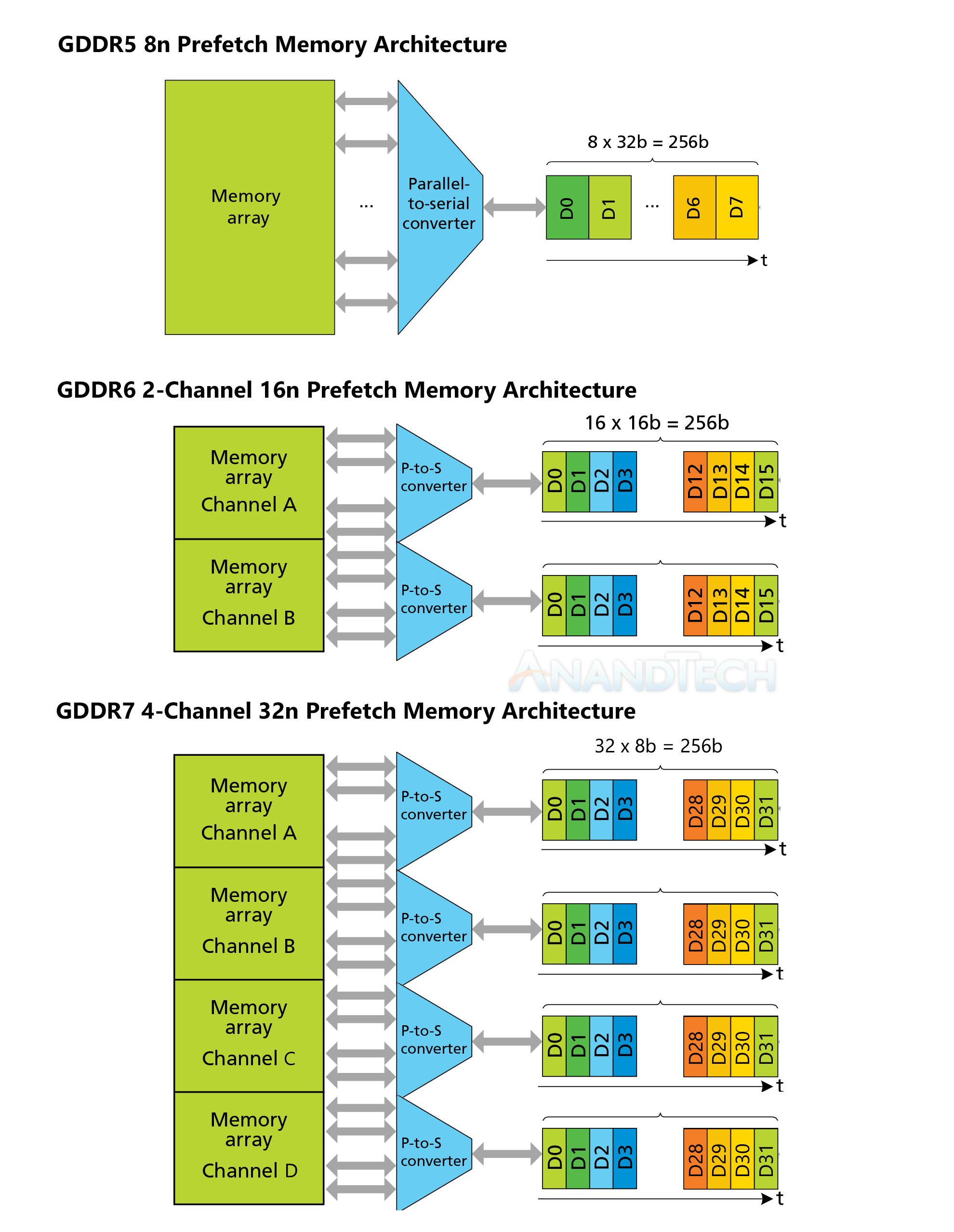
GDDR Channel Architecture. Original GDDR6-era Diagram Courtesy Micron
The net impact of all of this is that, by halving the channel width but keeping the prefetch size the same, JEDEC has effectively doubled the amount of data that is prefetched per cycle of the DRAM cells. This is a pretty standard trick to extend the bandwidth of DRAM memory, and is essentially the same thing JEDEC did with GDDR6 in 2018. But it serves as a reminder that DRAM cells are still very slow (on the order of hundreds of MHz) and aren't getting any faster. So the only way to feed faster memory buses is by fetching ever-larger amounts of data in a single go.
The change in the number of channels per memory chip also has a minor impact on how multi-channel "clamshell" mode works for higher capacity memory configurations. Whereas GDDR6 accessed a single memory channel from each chip in a clamshell configuration, GDDR7 will access two channels – what JEDEC is calling two-channel mode. Specifically, this mode reads channels A and C from each chip. It is effectively identical to how clamshell mode behaved with GDDR6, and it means that while clamshell configurations remain supported in this latest generation of memory, there aren't any other tricks being employed to improve memory capacity beyond ever-increasing memory chip densities.
On that note, the GDDR7 standard officially adds support for 64Gbit DRAM devices, twice the 32Gbit max capacity of GDDR6/GDDR6X. Non-power-of-two capacities continue to be supported as well, allowing for 24Gbit and 48Gbit chips. Support for larger memory chips further pushes the maximum memory capacity of a theoretical high-end video card with a 384-bit memory bus to as high as 192GB of memory – a development that would no doubt be welcomed by datacenter operators in the era of large language AI models. With that said, however, we're still regularly seeing 16Gbit memory chips used on today's memory cards, even though GDDR6 supports 32Gbit chips. Coupled with the fact that Samsung and Micron have already disclosed that their first generation of GDDR7 chips will also top out at 16Gbit/24Gbit respectively, it's safe to say that 64Gbit chips are pretty far off in the future right now (so don't sell off your 48GB cards quite yet).
For their latest generation of memory technology, JEDEC is also including several new-to-GDDR memory reliability features. Most notably, on-die ECC capabilities, similar to what we saw with the introduction of DDR5. And while we haven't been able to get an official comment from JEDEC on why they've opted to include ECC support now, its inclusion is not surprising given the reliability requirements for DDR5. In short, as memory chip densities have increased, it has become increasingly hard to yield a "perfect" die with no flaws; so adding on-chip ECC allows memory manufacturers to keep their chips operating reliably in the face of unavoidable errors.
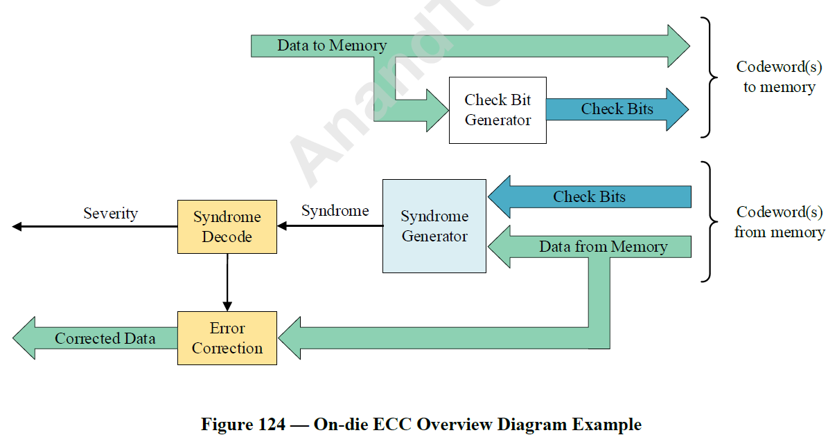
This figure is reproduced, with permission, from JEDEC document JESD239, figure 124
Internally, the GDDR7 spec requires a minimum of 16 bits of parity data per 256 bits of user data (6.25%), with JEDEC giving an example implementation of a 9-bit single error correcting code (SEC) plus a 7-bit cyclic redundancy check (CRC). Overall, GDDR7 on-die ECC should be able to correct 100% of 1-bit errors, and detect 100% of 2-bit errors – falling to 99.3% in the rare case of 3-bit errors. Information about memory errors is also made available to the memory controller, via what JEDEC terms their on-die ECC transparency protocol. And while technically separate from ECC itself, GDDR7 also throws in another memory reliability feature with command address parity with command blocking (CAPARBLK), which is intended to improve the integrity of the command address bus.
Otherwise, while the inclusion of on-die ECC isn't likely to have any more of an impact on consumer video cards than its inclusion had for DDR5 memory and consumer platforms there, it remains to be seen what this will mean for workstation and server video cards. The vendors there have used soft ECC on top of unprotected memory for several generations now; presumably this will remain the case for GDDR7 cards as well, but the regular use of soft ECC makes things a lot more flexible than in the CPU space.
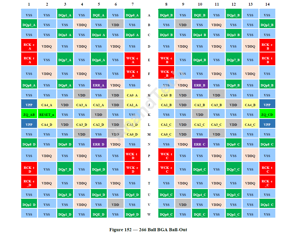
This figure is reproduced, with permission, from JEDEC document JESD239, figure 152
Finally, GDDR7 is also introducing a suite of other reliability-related features, primarily related to helping PAM3 operation. This includes core independent LFSR (linear-feedback shift register) training patterns with eye masking and error counters. LFSR training patterns are used to test and adjust the interface (to ensure efficiency), eye masking evaluates signal quality, and error counters track the number of errors during training.
Technical matters aside, this week's announcement includes statements of support from all of the usual players on both sides of the isle, including AMD and NVIDA, and the Micron/Samsung/SKhynix trifecta. It goes without saying that all parties are keen to getting to use or sell GDDR7 respectively, given the memory capacity and bandwidth improvements it will bring – and especially in this era where anything aimed at the AI market is selling like hotcakes.
No specific products are being announced at this time, but with Samsung and Micron having previously announced their intentions to ship GDDR7 memory this year, we should see new memory (and new GPUs to pair it with) later this year.
JEDEC standards and publications are copyrighted by the JEDEC Solid State Technology Association. All rights reserved.


10 Comments
View All Comments
meacupla - Wednesday, March 6, 2024 - link
I am eagerly awaiting for 3GB density to arrive.128bit memory bus GPUs don't have enough VRAM with 8GB, but they also don't have enough raster to fully utilize 16GB. Give them 3GB chips and they will have 12GB.
The same story with 192bit memory bus. Not enough VRAM with 12GB, but they will never have enough raster for 24GB. If they had 18GB from 6x3GB, that'd be more than enough.
ET - Thursday, March 7, 2024 - link
I agree about the notion of 3GB helping in this respect, though I the talk about "enough raster" seems irrelevant. If this arrives it will be with next gen cards, which will have higher bandwidth (thanks to GDDR7) and higher performance. So higher density RAM (or clamshell) will pretty much be needed to provide a decent amount of RAM to what will be low end cards which are equivalent to current mid-range ones, or mid range equivalent to high end.Threska - Wednesday, March 6, 2024 - link
"It goes without saying that all parties are keen to getting to use or sell GDDR7 respectively, given the memory capacity and bandwidth improvements it will bring – and especially in this era where anything aimed at the AI market is selling like hotcakes."Combined with this there should be more bang for the buck.
https://youtu.be/nP5pztB6wPU
NextGen_Gamer - Thursday, March 7, 2024 - link
I know AMD has confirmed that RDNA-4 is on track still for 2024 release, and it seems a given it will support GDDR7, but has anyone seen info on NVIDIA's next cards? I know the B100/AI version of "Blackwell" is 100% releasing this year (as NV has told investors on more than one occasion), but I don't think I've heard about the GPU/consumer versions as much.meacupla - Thursday, March 7, 2024 - link
Only nvidia is reserving GDDR7 right now, so RTX 5090 is most likely going to be GDDR7RDNA 4 is going to be Q3/Q4 with GDDR6 most likely.
https://www.youtube.com/watch?v=ZpjBHwfIyXs
Dante Verizon - Friday, March 8, 2024 - link
No one can say that. Your source is prone to low reliabilitykn00tcn - Saturday, March 9, 2024 - link
any examples of that low reliability? companies can change plans if the leak is early enough, and the leak is only as good as how familiar the original source contact is with the topic (who may be in a different department from the topic), so reliability increases when multiple contact quotes are listed and sometimes he lists the confidence levelSantoval - Sunday, March 10, 2024 - link
It is interesting they chose the more conservative PAM3 instead of DDR6X's PAM4. The latter would have doubled bandwidth, clock for clock, but it would require more quite robust error correction than PAM3.I think the switch to PAM is the primary reason for the on-die ECC.
PCIe 6.0 uses PAM4, the first PCIe version based with PAM signaling. Which is why it requires heavy-duty error correction.
Santoval - Sunday, March 10, 2024 - link
p.s./edit: Sorry, I meant "GDDR6X".KAlmquist - Tuesday, March 12, 2024 - link
So the idea is that memory errors are corrected on chip, and transfer errors are corrected buy the GPU memory controller. That avoids the case where a bit is flipped in memory and then the data is further corrupted during transfer to the GPU, resulting in the data seen by the GPU being too badly corrupted to be fixed.