Original Link: https://www.anandtech.com/show/6292/iphone-5-a6-not-a15-custom-core
The iPhone 5's A6 SoC: Not A15 or A9, a Custom Apple Core Instead
by Anand Lal Shimpi on September 15, 2012 2:15 PM EST- Posted in
- Apple
- Smartphones
- Mobile
- SoCs
- iPhone 5
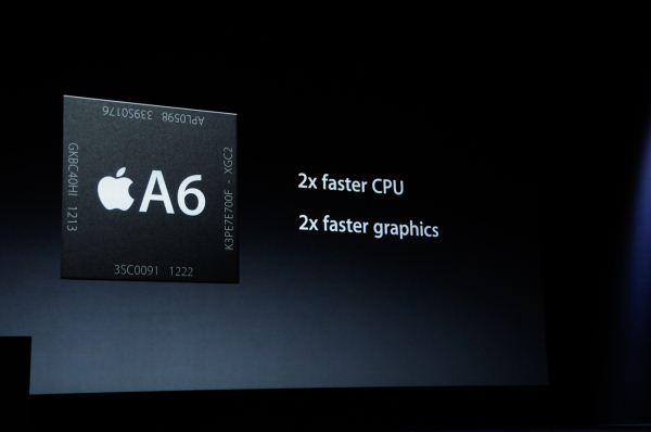
When Apple announced the iPhone 5, Phil Schiller officially announced what had leaked several days earlier: the phone is powered by Apple's new A6 SoC.
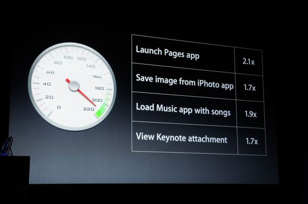
As always, Apple didn't announce clock speeds, CPU microarchitecture, memory bandwidth or GPU details. It did however give us an indication of expected CPU performance:
Prior to the announcement we speculated the iPhone 5's SoC would simply be a higher clocked version of the 32nm A5r2 used in the iPad 2,4. After all, Apple seems to like saving major architecture shifts for the iPad.
However, just prior to the announcement I received some information pointing to a move away from the ARM Cortex A9 used in the A5. Given Apple's reliance on fully licensed ARM cores in the past, the expected performance gains and unpublishable information that started all of this I concluded Apple's A6 SoC likely featured two ARM Cortex A15 cores.
It turns out I was wrong. But pleasantly surprised.
The A6 is the first Apple SoC to use its own ARMv7 based processor design. The CPU core(s) aren't based on a vanilla A9 or A15 design from ARM IP, but instead are something of Apple's own creation.
Hints in Xcode 4.5
The iPhone 5 will ship with and only run iOS 6.0. To coincide with the launch of iOS 6.0, Apple has seeded developers with a newer version of its development tools. Xcode 4.5 makes two major changes: it drops support for the ARMv6 ISA (used by the ARM11 core in the iPhone 2G and iPhone 3G), keeps support for ARMv7 (used by modern ARM cores) and it adds support for a new architecture target designed to support the new A6 SoC: armv7s.
What's the main difference between the armv7 and armv7s architecture targets for the LLVM C compiler? The presence of VFPv4 support. The armv7s target supports it, the v7 target doesn't. Why does this matter?
Only the Cortex A5, A7 and A15 support the VFPv4 extensions to the ARMv7-A ISA. The Cortex A8 and A9 top out at VFPv3. If you want to get really specific, the Cortex A5 and A7 implement a 16 register VFPv4 FPU, while the A15 features a 32 register implementation. The point is, if your architecture supports VFPv4 then it isn't a Cortex A8 or A9.
It's pretty easy to dismiss the A5 and A7 as neither of those architectures is significantly faster than the Cortex A9 used in Apple's A5. The obvious conclusion then is Apple implemented a pair of A15s in its A6 SoC.
For unpublishable reasons, I knew the A6 SoC wasn't based on ARM's Cortex A9, but I immediately assumed that the only other option was the Cortex A15. I foolishly cast aside the other major possibility: an Apple developed ARMv7 processor core.
Balancing Battery Life and Performance
There are two types of ARM licensees: those who license a specific processor core (e.g. Cortex A8, A9, A15), and those who license an ARM instruction set architecture for custom implementation (e.g. ARMv7 ISA). For a long time it's been known that Apple has both types of licenses. Qualcomm is in a similar situation; it licenses individual ARM cores for use in some SoCs (e.g. the MSM8x25/Snapdragon S4 Play uses ARM Cortex A5s) as well as licenses the ARM instruction set for use by its own processors (e.g. Scorpion/Krait implement in the ARMv7 ISA).
For a while now I'd heard that Apple was working on its own ARM based CPU core, but last I heard Apple was having issues making it work. I assumed that it was too early for Apple's own design to be ready. It turns out that it's not. Based on a lot of digging over the past couple of days, and conversations with the right people, I've confirmed that Apple's A6 SoC is based on Apple's own ARM based CPU core and not the Cortex A15.
Implementing VFPv4 tells us that this isn't simply another Cortex A9 design targeted at higher clocks. If I had to guess, I would assume Apple did something similar to Qualcomm this generation: go wider without going substantially deeper. Remember Qualcomm moved from a dual-issue mostly in-order architecture to a three-wide out-of-order machine with Krait. ARM went from two-wide OoO to three-wide OoO but in the process also heavily pursued clock speed by dramatically increasing the depth of the machine.
The deeper machine plus much wider front end and execution engines drives both power and performance up. Rumor has it that the original design goal for ARM's Cortex A15 was servers, and it's only through big.LITTLE (or other clever techniques) that the A15 would be suitable for smartphones. Given Apple's intense focus on power consumption, skipping the A15 would make sense but performance still had to improve.
Why not just run the Cortex A9 cores from Apple's A5 at higher frequencies? It's tempting, after all that's what many others have done in the space, but sub-optimal from a design perspective. As we learned during the Pentium 4 days, simply relying on frequency scaling to deliver generational performance improvements results in reduced power efficiency over the long run.
To push frequency you have to push voltage, which has an exponential impact on power consumption. Running your cores as close as possible to their minimum voltage is ideal for battery life. The right approach to scaling CPU performance is a combination of increasing architectural efficiency (instructions executed per clock goes up), multithreading and conservative frequency scaling. Remember that in 2005 Intel hit 3.73GHz with the Pentium Extreme Edition. Seven years later Intel's fastest client CPU only runs at 3.5GHz (3.9GHz with turbo) but has four times the cores and up to 3x the single threaded performance. Architecture, not just frequency, must improve over time.
At its keynote, Apple promised longer battery life and 2x better CPU performance. It's clear that the A6 moved to 32nm but it's impossible to extract 2x better performance from the same CPU architecture while improving battery life over only a single process node shrink.
Despite all of this, had it not been for some external confirmation, I would've probably settled on a pair of higher clocked A9s as the likely option for the A6. In fact, higher clocked A9s was what we originally claimed would be in the iPhone 5 in our NFC post.
I should probably give Apple's CPU team more credit in the future.
The bad news is I have no details on the design of Apple's custom core. Despite Apple's willingness to spend on die area, I believe an A15/Krait class CPU core is a likely target. Slightly wider front end, more execution resources, more flexible OoO execution engine, deeper buffers, bigger windows, etc... Support for VFPv4 guarantees a bigger core size than the Cortex A9, it only makes sense that Apple would push the envelope everywhere else as well. I'm particularly interested in frequency targets and whether there's any clever dynamic clock work happening. Someone needs to run Geekbench on an iPhone 5 pronto.
I also have no indication how many cores there are. I am assuming two but Apple was careful not to report core count (as it has in the past). We'll get more details as we get our hands on devices in a week. I'm really interested to see what happens once Chipworks and UBM go to town on the A6.
The A6 GPU: PowerVR SGX 543MP3?
Apple made a similar "up to 2x" claim for GPU performance. It didn't share any benchmarks, but there are four options here:
1) PowerVR SGX 543MP2 (same as in A5) at 2x the clock speed
2) PowerVR SGX 543MP4 at the same clock as the MP2 in the A5
3) Marginally higher clocked PowerVR SGX 543MP3
4) Next-gen PowerVR Rogue GPU
It's too early for #4. The first option makes sense but you run into the same issues as on the CPU side with higher voltages used to ramp clocks up (also possible that you drop voltages in the move to the new process technology).
The second option trades voltage for die area, which based on the A5X Apple is clearly willing to spend where necessary.
The third is sort of the best of both worlds. You don't take a huge die area penalty and at the same time don't run at a significantly higher frequency, and you can get to that same 2x value.
The third option is the most elegant and likely what Apple chose here. Remember that overall die size is dictated by the amount of IO you have around the chip. The A5X had four 32-bit LPDDR2 memory controllers, which gave Apple a huge die area to work with. The move to a smaller manufacturing process cuts down the total die area, which means Apple would either have to add a ton of compute (to fill empty space, no sense in shipping a big chip with a bunch of unused area) or reduce the memory interface to compensate. Pair that knowledge with the fact that Apple doesn't have the same memory bandwidth requirements on the iPhone 5 (0.7MP vs. 3.1MP display) and it makes sense that Apple would go for a narrower memory interface with the A6 compared to the A5X.
How much narrower? Phil Schiller mentioned the A6 was 22% smaller than the A5. We can assume this is compared to the 45nm A5 and not the 32nm A5r2, which would mean that we don't have any more memory channels compared to the A5. In other words, it's quite likely the A6 has a 2x32-bit LPDDR2 memory interface once again.
Final Words
There's not much more to add for now. We'll have a device in a week and I suspect the first reviews will be out a day or two before then. Then the real work begins on finding out exactly what Apple has done inside the A6. If anyone has been dying to put together some good low level iOS benchmarks, now is the time to start.
This is a huge deal for Apple. It puts the company in another league when it comes to vertical integration. The risks are higher (ARM's own designs are tested and proven across tons of different devices/platforms) but the payoff is potentially much greater. As Qualcomm discovered, it's far easier to differentiate (and dominate?) if you're shipping IP that's truly unique from what everyone else has.
Now we get to see just how good Apple's CPU team really is.


